- 您现在的位置:买卖IC网 > Sheet目录1219 > HI2303EVAL1 (Intersil)EVALUATION BOARD HI2303
�� �
�
�Application� Note� 9783�
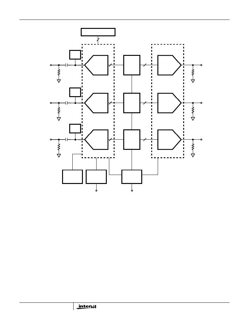
�CONTROL� SWITCHES�
�8�
�BIAS�
�TEE�
�HI-2303�
�HI-3050�
�A� IN�
�0.1� μ� F�
�CHANNEL� 1�
�ADC�
�8�
�DATA�
�LATCHES�
�8�
�CHANNEL� 1�
�DAC�
�A� OUT�
�75�
�BIAS�
�TEE�
�75�
�B� IN�
�0.1� μ� F�
�CHANNEL� 2�
�ADC�
�8�
�DATA�
�LATCHES�
�8�
�CHANNEL� 2�
�DAC�
�B� OUT�
�75�
�BIAS�
�TEE�
�75�
�C� IN�
�0.1� μ� F�
�CHANNEL� 3�
�ADC�
�8�
�DATA�
�LATCHES�
�8�
�CHANNEL� 3�
�DAC�
�C� OUT�
�75�
�75�
�VOLTAGE�
�REFERENCE�
�CLAMP�
�DRIVER�
�CLAMP� IN�
�CLOCK�
�DRIVER�
�CLOCK� IN�
�FIGURE� 1.� FUNCTIONAL� BLOCK� DIAGRAM�
�Buffered� Clock� Driver�
�In� order� to� ensure� rated� performance� of� the� HI2303,� the� duty�
�cycle� of� the� sample� clock� should� be� set� to� 50%.� It� must� also�
�have� low� phase� noise� and� operate� at� standard� TTL� logic� levels.�
�It� can� be� dif?cult� to� ?nd� a� low� phase� noise� generator� that� will�
�provide� a� 50MHz� squarewave� at� TTL� logic� levels.� Conse-�
�quently,� the� evaluation� board� is� designed� with� a� logic� buffer�
�(U2)� acting� as� a� voltage� comparator� to� generate� the� sam-�
�pling� clock� for� the� HI2303� when� a� sinewave� (<� ±� 1.5V)� is�
�applied� to� the� CLK� input� of� the� evaluation� board.� The� sample�
�clock� sinewave� is� AC� coupled� into� the� input� of� the� inverter�
�and� a� discrete� bias� tee� is� used� to� bias� the� sinewave� around�
�the� trigger� level� of� the� inverter’s� input.� The� variable� resistor�
�varies� the� DC� bias� voltage� added� to� the� sinewave� input�
�allowing� the� user� to� adjust� the� duty� cycle� of� the� sampling�
�clock� to� obtain� the� best� performance� from� the� ADC� and� to�
�evaluate� the� effects� of� sample� clock� duty� cycle� on� the� perfor-�
�mance� of� the� converter.� The� sinewave� to� logic� level� compar-�
�2�
�ator� drives� a� series� of� additional� buffers� that� provides�
�isolation� between� the� three� sample� clocks� used� on� the� eval-�
�uation� board.� One� clock� drives� the� ADC� clock� input� pin�
�(AD_CLOCK),� a� second� clock� drives� output� data� latches�
�(LATCH_CLOCK),� and� the� last� clock� provides� the� DAC�
�reconstruct� clock(DA_CLOCK).�
�Reconstruction� DAC�
�To� easily� verify� the� performance� of� the� ADC� a� reconstruction�
�DAC� is� provided.� The� 10-bit� HI3050� triple� DAC� was� selected�
�to� ensure� the� user� measures� the� real� ADC� performance�
�without� any� degradation� from� the� reconstruct� DAC.� The� DAC�
�is� con?gured� to� convert� the� latched� data� into� a� 2V� fullscale�
�output.� The� fullscale� output� can� be� adjusted� slightly� via� R9.�
�The� DAC� is� optimized� for� the� fullscale� output� voltage� of� 1.8�
�to� 2.0V� so� care� should� be� exercised� when� operating� outside�
�of� the� designed� range.�
�发布紧急采购,3分钟左右您将得到回复。
相关PDF资料
HI3026EVAL
EVALUATION PLATFORM HI3026
HI5746EVAL1
EVALUATION PLATFORM HI5746
HIP1011AEVAL1
EVAL BOARD PCI HOT PLUG HIP1011
HIP1011DEVAL1
EVAL BOARD PCI HOT PLUG DUAL
HIP1011EVAL1
PCI HOT PLUG EVALUATION BOARD
HIP1011EVAL2
EVAL BOARD COMPACT PCI HOT PLUG
HIP1012EVAL1
EVALUATION BOARD DUAL GENERIC
HIP1013EVAL1
EVALUATION BOARD DUAL GENERIC
相关代理商/技术参数
HI2303JCQ
制造商:Rochester Electronics LLC 功能描述:80 PQFP INDTEMP TRIPLE A/D 8BIT 50MSPS D - Bulk
HI2304
制造商:INTERSIL 制造商全称:Intersil Corporation 功能描述:Triple 8-Bit, 20 MSPS, RGB, 3-Channel D/A Converter
HI2-304-2
制造商:未知厂家 制造商全称:未知厂家 功能描述:SPST Analog Switch
HI2-304-5
制造商:未知厂家 制造商全称:未知厂家 功能描述:SPST Analog Switch
HI2304JCQ
制造商:INTERSIL 制造商全称:Intersil Corporation 功能描述:Triple 8-Bit, 20 MSPS, RGB, 3-Channel D/A Converter
HI2-305-2
制造商:未知厂家 制造商全称:未知厂家 功能描述:SPDT Analog Switch
HI2-305-5
制造商:未知厂家 制造商全称:未知厂家 功能描述:SPDT Analog Switch
HI2307
制造商:INTERSIL 制造商全称:Intersil Corporation 功能描述:Triple 10-Bit, 50 MSPS, RGB, 3-Channel D/A Converter